IBM sub-1nm chip breakthrough hinges on ASML High-NA tools
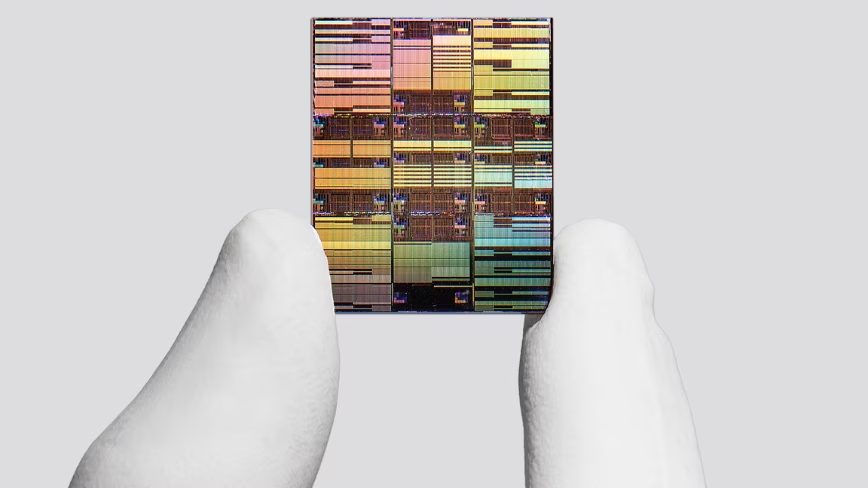
IBM has demonstrated a sub-1nm transistor architecture, a five-year-out research milestone that signals the semiconductor industry will ultimately need ASML’s expensive High-NA lithography machines to keep scaling.
IBM has built a working transistor architecture it calls the 0.7nm, or 7-angstrom, node. The design packs nearly 100 billion transistors onto a piece of silicon the size of a fingernail.
That density is almost twice that of the 2nm chip IBM unveiled in 2021. Rather than shrinking transistors on a flat plane, IBM’s "nanostack" design stacks them vertically, allowing engineers to tune the power and performance of each layer independently using different material combinations.
IBM projects the new node offers up to 50% more performance or 70% better energy efficiency than its 2nm generation, though these figures represent different operating points in a lab setting. Crucially, the architecture also achieves a 40% scaling reduction in SRAM, the fast on-chip memory that has proven stubborn to shrink and is vital for artificial intelligence workloads.
This is not merely a simulation. IBM told the VLSI 2026 conference it validated the structure through dielectric bonding and demonstrated a working CMOS inverter. “With our new nanostack architecture, we’re not just making smaller transistors, we’re reinventing how chips are built,” said Jay Gambetta, director of IBM Research.
The ASML connection
For European investors, the equipment behind the work matters as much as the physics. IBM developed the nanostack at its Albany research complex in New York alongside partners Lam Research, Tokyo Electron, and SCREEN Semiconductor Solutions. That facility is slated to soon house a next-generation High-NA EUV lithography tool from ASML, the Dutch firm that holds a global monopoly on machines required to print circuits this small.
The announcement effectively serves as a research validation for ASML’s expensive new tools, which have divided the industry. TSMC, the world’s dominant chipmaker, has initially been sceptical of adopting the technology due to its price.
There are significant caveats to the milestone. The "0.7nm" label is a generational marker rather than a literal physical measurement of the transistor features. IBM sold its manufacturing operations to GlobalFoundries in 2014 and now only develops technology to be licensed and built by others. The company estimates the path to commercial production is at least five years away, giving the industry a long runway to resolve its disputes over the economics of High-NA lithography.